CS641 Class
17
Note hw5,
due next Mon.
Last time: Combinational
circuits: using gates to do specified logical calculations
Read:
Appendix C, on CD-ROM, logic handout linked from syllabus
Combinational Logic
° Complex logic blocks are built from AND, OR, NOT (or another set of basic gates).
° A combinational logic block is one in which the output is a function only of its current input.
° Combinational logic cannot have memory (e.g., a register is not a combinational unit). More about memory later…
Review: look at common
larger combinational blocks:
2-Input Multiplexor (MUX): controls which input gets
through
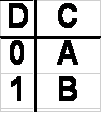

That’s not really a “truth table” though, need to show what happens with all 3 inputs: see notes of 3/23.
General Multiplexors:
• have control bits and data bits
• control bits select which data bit will pass through: all others are blocked
•
in
general,
1 control bit selects between 2 data bits,
2 control bits select between 4 data
bits,
3 control bits select between 8 data bits,
n control bits select between 2n data bits
so we can build a mux of any size to serve our
purpose
Using MUXes
° Used to select one of N different inputs, for ex., in CPU
Another Important Combinational Circuit: Decoder
The inputs say which output number to make 1, rest 0
i.e., if A,B is a code, it specifies which
outbound device to activate (say). Again, used in CPU.


So how do we implement combinational logic?
Combinational Logic
° Any combinatorial logic block, not matter how complex can be written as a OR of many ANDs using NOTs
° Called “sum-of-products”in Boolean algebra
• Sum à boolean OR
• Product à boolean AND
° Can convert any truth table to sum-of-product form
Simplistic approach:
write a product (ANDs) for each line in the truth table, then sum (OR) all the
products
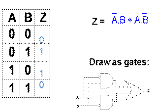
Example: Exclusive OR
“Exclusive or”
(XOR). True if the two inputs are the different, false if the two inputs are
same
There are XOR gates,
but let’s construct XOR out of OR, AND, and NOT.
We write out the truth
table, then look for 1’s in ouput Z, write sum of products:
Taking advantage of sum-of-products
° Since sum-of-products is a convenient notation and way to think about design, offer hardware building blocks that match that notation
° One example is Programmable Logic Arrays (PLAs)—will look at later
NAND Gates: a “Universal Gate”


A. You replace an NOT
gate
with 1 or more NAND gates
B. You replace a AND gate
with 1 or more NAND gates
C. You replace an OR gate
with 1 or more NAND gates
D. You replace NOT and AND
E. You replace NOT, AND, OR
° ISA (instruction set architecture) is very important abstraction layer
• Contract between HW and SW
° Basic building blocks are logic gates
° Clocks control pulse of our circuits
° Two types
• Stateless Combinational Logic (&,|,~), in which output is function of input only (no memory)
• State circuits (e.g., registers)
Hw5 introduces R-S Flipflop, most primitive state-holding circuit
Sequential Circuits Overview

° Sequential circuits have feedback, e.g.
° Output is function of inputs + fed-back signals.
° Feedback signals are critical to holding the circuit's state.
° Assuming optimized design, the feedback signals are one-one with the bits held in the device.
° It’s something like when you keep repeating something to yourself to keep from forgetting it—the held data is alive in the circuit
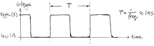
Clocks ![]()
° A clock determines when the circuit changes states.
° Produces discrete updating, so we have state at “time” 0, time 1, …
° It's really a signal:
•
high=1, low=0,
quick changes from one to the other
• state changes occur on the “edges”: rising edge, falling edge (also see Fig. C.7.1)
° Period = time between ticks (if same every time, anyway) = T
° Frequency = 1/T
°
Real life:
There’s a Clock input to each Sequential Circuit, whether or not shown.
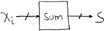
State Elements Handout: Considers how to add up numbers that are supplied on each clock cycle.
Uses a register to hold the running sum.
Registers
We have been using CPU registers: know they hold 32-bit quantities.
Now look at them as a hardware device:
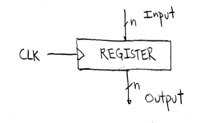
Inside the register: 32 flip-flops. You can put some dots in the box to represent the bits being held by flip-flops inside.
Question: where is the feedback?
Answer: inside the flip-flops. We now take the flip-flop as given, a building block.
How it works:
Load register with x: put x bits on Input. When the clock falling edge occurs, the register accepts x and expresses it on Output pins after a tiny delay. Then it holds that value and ignores the input until the next falling edge.
Note how the register takes a snapshot of the input at the moment of the falling edge. This is a very nice property that makes it easy to reason about how it works in a circuit.
Read register: After a few nanoseconds, use Output value as desired. They will be good until the next clock falling edge, including the moment of the next falling edge.
Now we’re ready to look at the State Elements handout linked to the Syllabus.
Accumulator Example
Given: a series of multibit values X0, X1, ..., , one valid at each clock falling edge of consecutive clock cycles.
Challenge: Add them up, provide their sum as multibit signal S.

Combinational element we need: an Adder, S = X + Y. Since S is a pure function of X and Y, this can be done in a combinational circuit, itself the component with the plus sign on it in the next diagram, but with X and Y coming into the two multibit inputs.
Plan A
feed the output of the adder back into itself to do the next addition:

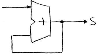
What happens?
Suppose S=0 to start and the gate delay in the adder is 1 ns and the clock period is 5 ns.
At the first clock falling edge, X0 and 0 are on the adder inputs, so S = X0.
One ns later, X0 and X0 are on the adder inputs, so S = 2*X0
One ns later, X0 and 2*X0 are on the adder inputs, so S = 3*X0
...
5 ns later, clock falls again, and by this time, X1 is on the upper input, so it starts getting added in multiple times.
This is out of control.
Even the startup is unclear here: how can we make S=0 to start?
Moral: don’t try to use feedback with just gates in your own design: leave it to the internals of flip-flops.
Plan B, the one that works:
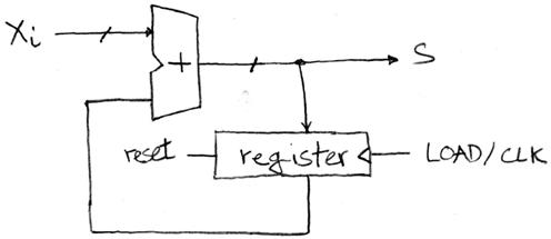
We wrote this out blow by blow, but that’s not how engineers express the history.
Note that the initial condition S=0 is obtainable by “clearing the register”, usually available by another pin (input) of the register.
Here’s the timing diagram:
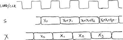
To understand this:
1. Mark the falling edges of the clock and drop dotted lines down from there.
2. Where the dotted lines cross the X values, that’s what gets sampled into the register.
3. Right after that, the S changes due to the addition.