Start Chap. 4 on the CPU
Note that the chapter is written so that readers can understand it without covering circuit theory, or very little about it. So there is some coverage that should be easy to read through. Try to read to Sec. 4.5 for next week.
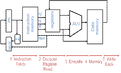
The CPU
° Processor (CPU): the active part of the computer, which does all the work (data manipulation and decision-making)
• Datapath: portion of the processor which contains hardware necessary to perform all operations required by the computer (the muscle)
• Control: portion of the processor (also in hardware) which tells the datapath what needs to be done (the brain)
See Figure 4.2 for
the basic setup, where the datapath elements are in
black and the control circuitry in blue.
Working from left to
right:
The PC contains the
address of the next instruction in instruction memory. Its value gets replaced
by PC+4 via the adder and MUX and the back arc. But the value PC+4 is also used
in branch instructions, along with a part of the instruction, shown coming out
of instruction memory on its right, and this also can replace the PC.
The instruction
coming out of instruction memory can also feed into a register in the register
set, and is input to Control.
The value of a
register can go to the ALU, and the other operand can come from a register or
part of the instruction.
The result from the
ALU goes back to a register, assuming it goes through the MUX.
The register value
also can go through to data memory (store), and data memory can supply a value
that goes to a register (load)
The state elements
are the two “memories” and the registers.
The ALU, adders and MUXes are all combinational. Thus we have characterized all
the elements in the datapath, leaving Control as a
black box.
Of course there is a
clock, and as stated on pg. 305, we are assuming edge-triggered components.
Sec. 4.3 Elaborates on the Datapath
elements and what gets used on
various MIPS instructions
Instruction memory
is treated as read-only memory, leaving out the loading of memory for now.
Consider an R-type
instruction like add $t1, $t2, $t3, which adds $t2 and $t3 and puts the sum in
$t1.
This reads two
registers from the register file, adds them in the ALU, and writes the result
back in the register file.
So do all the other
R-format instructions.
This ALU does the
needed operation (based on control inputs), and outputs the result and Zero,
the result-is-0 signal.
Sec. 4.4 Shows how it’s possible
to implement a “single-cycle” CPU out of this plan
Instructions
supported: lw, sw, beq, add, sub, and, or, slt (set on less than).
The ALU can do 6
operations, controlled by 4 bits, as shown on pg. 216
These 4 bits can be
generated from 2 bits from the “main control unit” and the instruction’s bits,
as shown by a truth table on pg. 217.
That means the main
control unit only needs to generate 2 bits to go to the ALU, a great
simplification.
See Fig. 4.17, pg.
322
We see Control needs
to generate several other signals as well.
These are all
outputs of the TT on pg. 323, with input from the instruction itself.
So Control is all
combinational here (single-cycle case!!)
We see that the ALU,
which also gets to see the funct field of the
instruction, only cares otherwise whether the instruction is load/store, R
format, or beq.
Knowing that Control
is combinational gives us the power to analyze the whole thing, since we have
previously studied the other units.
Note: Recall that the register file works differently on
read and write:
The register reading is not “clocked”. When you ask to read register 6, you get your wires connected to that internal reg (register).
But the register
writing is clocked: need to have the clock edge involved.
So basically, the
register file and memories here read like combinational circuits. No clock
needed.
So looking again at
pg. 322, which shows the datapath for add, etc.
PC stable -->
read instruction --> Control -->select registers --> inputs to ALU,
control says read --> apply inserts to register file for result
all without needing a clock
Finally, to write
the result into a register, need to wait for the clock. At same time, have set
up next PC
SO at clock edge,
write result into register and get new PC value
Similarly other
instructions
load
PC stable -->
read instruction --> Control -->select dst reg, RegOut, read-data from mem, so mem data routed to reg file
Clock edge: read
data in to reg, next PC
And so on
But as said on pg.
328, this is not really the way to go—the clock cycle is too long.
Need pipelining, Sec. 4.5
Look at laundry
example, pg. 331 (errata: add gray boxes in timeline for “storer”
steps)
°
Problem:
a single, atomic block which “executes an instruction” (performs all necessary
operations beginning with fetching the instruction) would be too bulky and
inefficient
°
Solution:
break up the process of “executing an instruction” into stages, and then
connect the stages to create the whole datapath
•
smaller
stages are easier to design
easier to optimize (change) one stage without
touching the others
Pipeline Stages for MIPS
°
Stage 1:
Instruction Fetch
•
no
matter what the instruction, the 32-bit instruction word must first be fetched
from memory (the cache-memory hierarchy)
•
also,
this is where we Increment PC
(that is, PC = PC + 4, to point to the next instruction: byte addressing so +
4)
°
Stage 2:
Instruction Decode
•
upon
fetching the instruction, we next gather data from the fields (decode
all necessary instruction data)
•
first,
read the Opcode to determine instruction type and
field lengths
•
second,
read in data from all necessary registers
°
for add,
read two registers
°
for addi, read one register
°
for jal, no reads necessary
°
Stage 3:
ALU (Arithmetic-Logic Unit)
•
the real
work of most instructions is done here: arithmetic (+, -, *, /), shifting,
logic (&, |), comparisons (slt)
•
what about loads
and stores?
°
lw $t0, 40($t1)
°
the
address we are accessing in memory = the value in $t1 + the value 40
°
so we do
this addition in this stage
°
Stage 4:
Memory Access
•
actually
only the load and store instructions do anything during this stage; the others
remain idle
•
since
these instructions have a unique step, we need this extra stage to account for
them
•
as a
result of the cache system, this stage is expected to be just as fast (on
average) as the others
°
Stage 5:
Register Write
•
most
instructions write the result of some computation into a register
•
examples:
arithmetic, logical, shifts, loads, slt
•
what about stores,
branches, jumps?
°
don’t
write anything into a register at the end
°
these
remain idle during this fifth stage
Pipeline Examples
°
add $r3,$r1,$r2 # r3 = r1+r2
•
Stage 1:
fetch this instruction, inc. PC
•
Stage 2:
decode to find it’s an add, then
read registers $r1 and $r2
•
Stage 3:
add the two values retrieved in
Stage 2
•
Stage 4:
idle (nothing to write to memory)
•
Stage 5:
write result of Stage 3 into
register $r3
°
sw $r3, 17($r1)
•
Stage 1:
fetch this instruction, inc. PC
•
Stage 2:
decode to find it’s a sw, then
read registers $r1 and $r3
•
Stage 3:
add 17 to value in register $r1
(retrieved in Stage 2)
•
Stage 4:
write value in register $r3
(retrieved in Stage 2 and
kept for this instruction) into memory
address computed in Stage 3
•
Stage 5:
go idle (nothing to write into a register)
•
Note the
mystery of keeping data for the
instruction across stages
°
Why does MIPS have five if instructions tend to go idle for at
least one stage?
There is one instruction that uses all five stages: the load
lw $r3,
17($r1)
•
Stage 1:
fetch this instruction, inc. PC
•
Stage 2:
decode to find it’s a lw, then
read register $r1
•
Stage 3:
add 17 to value in register $r1
(retrieved in Stage 2)
•
Stage 4:
read value from memory
address compute in Stage 3
•
Stage 5:
write value found in Stage 4 into
register $r3
•
Note
that all stages are in use here

°
Construct datapath
based on register transfers required to perform instructions
°
Control path causes the right transfers to
happen
Look at datapath in terms of
stages: like pg. 345
°
°
Now we’ll
use a finite state machine for control
°
Break up
the instructions into steps, each step takes a cycle
°
balance
the amount of work to be done
°
restrict
each cycle to use only one major functional unit
°
At the
end of a cycle
°
store
values for use in later cycles (easiest thing to do)
°
introduce
additional “internal” registers
°
See pg.
347 for the pipeline registers
°
This is
how data is held across stages for an individual instruction